Lithography
FSM provides a wide variety of wafer patterning solutions catered to the semiconductor and MEMS industries. Standard test patterns are available for CMP, Etch, Clean, and Medical Device manufacturing markets on glass and silicon substrates. In addition to our standard test pattern offerings, FSM accepts custom wafer patterning projects based upon end-user design with an option to provide engineering CAD and mask manufacture.
Materials: Silicon, Glass
Wafer Diameters: 50mm to 300mm
Lithography Tools: Scanner, Stepper, Proximity/contact aligner, E-Beam
Technology Nodes: 65nm, 90nm, 130nm, 180nm, 250nm and larger
Photoresist: 193nm, 248nm(DUV), I-Line
Etch: Wet, RIE, DRIE
CMP: W, Cu, Al, Oxide, TEOS
Metrology: SEM, Cross Section, E- Test etc.
Test Reticles:
TSV wafers
CMP Dishing and Erosion
Surface Trench Isolation (STI)
Damascene and Dual Damascene
Line /Space Arrays
Via Arrays
Daisy Chain
Memory Patterns
E-testable structures
Specialty Products: :
Precious Metals: Au, Pd, Ag, Pt
Thick Photoresist
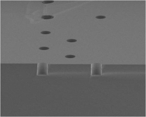
TSV 100 SiVia
FSM offers Through-Silicon Via (TSV) wafers with a via depth of 100um and a diameter of 50um.
The Through-Silicon Via (TSV) is etched with excellent sidewall surface roughness from the center of the wafer to the edge of the wafer aligned to the notch.
All Through Silicon Vias are etched on a 10 to 100um Via Etch Pattern Layout for a 200mm wafer.
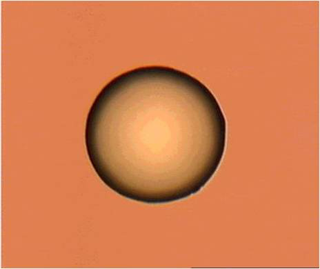
The electroplated copper layer is 10,000 angstroms followed by 2um Cu seed layer and 1000 angstroms Titanium Liner on TEOS.
Cross Section
Si vias, before Cu seed
 aft. Cu seed
Please
CONTACT FSM for more information.

 简体中文
简体中文 Japanese(日语)
 Korean(韩文)
 English(英文)